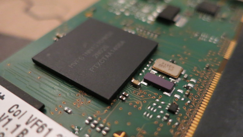
Freescale Vybrid SoC
In preparation to my talk at BetterEmbedded I had a deeper look into the second core of Freescales Vybrid VF6xx SoC. I wanted to create a bare-metal test firmware for the Cortex-M4 processor. As the Cortex-M4 is a companion of the Cotex-A5 in the same SoC, its boot process is different compared to a normal Microcontroller (e.g. STM32F4 or similar). Microcontroller usually boot directly from memory mapped NOR flash.
ARM SoCs in general contain a small, internal boot ROM where the cores start from. This boot ROM then tries to boot from different devices, such as NAND or SD-Card. For the Vybrid SoCs normally the Cotex-A5 is the boot CPU, which in my case is running Linux from NAND (the Timesys BSP). On startup, the Cortex-M4 is in an unclocked state and need to be started from the Linux side. With the Timesys BSP, a Vybrid specific kernel module called mcc is provided. This kernel module not only implements the Multi-Core Communication library but also allows to load an image into RAM and start the secondary CPU. The utility mqxboot allows to access this functionality from userspace. This components implement the boot procedure for the Cortex-M4 described in chapter 19.11, “Running Secondary Core”, of the Vybrid Reference Manaul.
The secondary core has not access to a NOR storage as it would have in a microcontroller. Instead the firmware runs completely from RAM.
Rather than really create something from scratch I opted to make use of libopencm3. libopencm3 is a open source (LGPL) library for various Cortex M3 and M4 devices. My plan is to add Vybrid (vf6xx) as another platform. First I updated the linker script in order to make sure the firmware will run the code from memory. In Vybrid, an internal RAM area called SRAM is suited for running the Cortex-M4 firmware from. This area has two access addresses, one which is used by the Cortex-M4 “Processor Code Bus” (PC-Bus, SRAM starting at 0x1f00000) and the “Processor System Bus” (PS-Bus, SRAM starting at 0x3f000000). Note this code aliases only exist for the Cortex-M4 core. The same memory is available from 0x3f000000 for the Cortex-A5. Right now I only make use of the PS-Bus.
I opted to put the vector addresses at the beginning of the SRAM area. Since the reset vector is not automatically read from 0x4, I opted to hard-code the code start section at an offset of 0x400 (see .text.reset_handler in the libopencm3_vf6xx.ld linker file). Some Vybrid specific startup code was also needed: The stack pointer, which is normally readed from 0x0, need to be initialized manually. This is done in the model specific pre_main function (see lib/vf6xx/vector_chipset.c). Then the vector table needs to be remapped to the start of the SRAM area. Finally we also want to make use of the floating point unit:
extern vector_table_t vector_table;
static inline void pre_main(void)
{
    /*
     * For Vybrid we need to set the stack pointer manually
     * since the boot ROM has its own stack
     */
    asm ( \
        "ldr sp,=_stack;" \
    );

    /* Set Vector Table Offset to our memory based vector table */
    SCB_VTOR = (uint32_t)&vector_table;

    /* Enable access to Floating-Point coprocessor. */
    SCB_CPACR |= SCB_CPACR_FULL * (SCB_CPACR_CP10 | SCB_CPACR_CP11);
}
With this, I was already able to run code on the M4. The easiest way to see if the Coretx-M4 core is really running is by incrementing a specific memory location and read this memory location from the Linux side (e.g. by using the user space utility devmem2). This quite unique debug feature comes in really handy: Read all memory in real time without having to mess around with JTAG and altering the run-time behavior is really useful 🙂
This initial port is available from my GitHub repository. I also plan to publish some demo code soon.
Furthermore I did some performance measurement when using different memory areas for code and data. Beside the mentioned aliases for the SRAM areas (aka. OCRAM, aka. sysRAM0/sysRAM1), there is also some tightly coupled SRAM (TCM, see Local Memory Controller in the reference manual). Two areas for code (starting at 0x1f800000) and data (starting at 0x3f80000) are available. I’m not sure yet whether this TCM SRAM is used by the L1 caches as well. The TCM RAM size is 2x32KiB, which does not match the mentioned 2x16KiB L1 caches. Also I could not run any code from the TCM RAM code area (starting at 0x3f80000), hence the empty line in the table below. All these measurement were done with L1 caches disabled. The raw measurement were done by incrementing an integer variable during 10 seconds. Those values would probably look quite different when running with L1 caches enabled and are neither scientific nor very meaningful for real-world scenarios…
| Data | |||||
|---|---|---|---|---|---|
| TCM (PS-Bus) | SRAM (PS-Bus) | TCM (PC-Bus) | SRAM (PC-Bus) | ||
| Code | TCM (PC-Bus) | 100.0% | 37.5% | 75.0% | 31.6% |
| SRAM (PC-Bus) | 30.0% | 30.0% | 35.3% | 20.7% | |
| TCM (PS-Bus) | |||||
| SRAM (PS-Bus) | 25.0% | 16.7% | 25.0% | 25.0% | |
Do you have any examples available for modification of the ld script in order to move code sections to TCM/SRAM-PC/SRAM-PS? I’m working with the gcc_cs toolchain which uses ld script instead of ARM .scat files and am trying to accomplish a relocation of critical code to TCML section for an M4 project.
Sorry for the late reply. This should be quite straight forward, have a look at the Linker file:
https://github.com/libopencm3/libopencm3-examples/blob/master/examples/vf6xx/colibri-vf61/colibri-vf61.ld
Just change the addresses after ORIGIN =, pc_ram is the memory location used for code, ps_ram is the memory location used for data (system).